Home→Interview Guides→Process Engineer (Semiconductor)
Process Engineer (Semiconductor) Interview Guide
Semiconductor process engineering in the Netherlands is entering a new phase. NXP and Nexperia operate established fabs; TSMC's planned European expansion will bring world-class volume manufacturing to the region. Process engineers who can bridge R&D and high-volume production are exceptionally sought after right now.
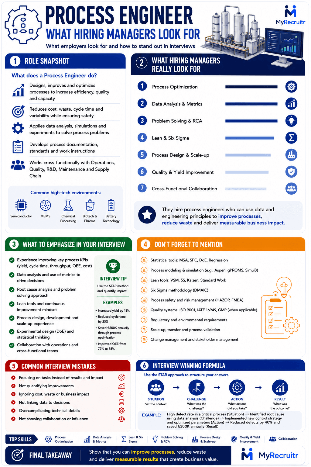
Got a vacancy for this role? Get tailored interview prep →
What hiring managers look for
Process module ownership: lithography, etch, deposition (CVD/PVD/ALD), CMP, diffusion, or implant
Statistical Process Control (SPC) and yield analysis — quantify yield improvements you have driven
Failure analysis skills: cross-section SEM, EDX, TEM sample preparation, root-cause methodology
Design of Experiments (DoE) for process optimisation — mention the specific methodology (Taguchi, RSM, full factorial)
Cleanroom experience and knowledge of contamination control protocols
Process integration awareness: understanding how your module interacts with adjacent process steps
Top priorities for this role
What hiring managers rank highest when screening Process Engineer (Semiconductor) candidates.
Process ownership — do you understand your process deeply enough to troubleshoot it at 2am without the process recipe in front of you?
Yield focus — can you analyse wafer maps, correlate with process history, and find root cause in data?
Cross-functional effectiveness — process engineering requires constant collaboration with equipment, integration, and yield engineering
Experimental design skills — can you design a DOE that efficiently identifies the critical process variables?
Safety in a hazardous chemical environment — semiconductor processes involve toxic, flammable, and corrosive chemicals
Common interview mistakes
Listing process steps without stating the technology node or product type (logic, DRAM, analogue, power)
No yield or throughput numbers — these are the language of fab management
Omitting equipment experience: tool types and vendors matter (Applied Materials, Lam Research, ASML, TEL)
Academic experience presented without clarity on whether it was research-grade or production-like conditions
Likely interview questions
Questions hiring managers commonly ask for Process Engineer (Semiconductor) roles in the Netherlands. Prepare concrete examples using the STAR method.
Q1
Walk me through how you would investigate a sudden yield drop on your process layer.
Q2
Describe a process optimisation project you led. What was the metric you were improving and how did you approach it?
Q3
How do you design a Design of Experiments (DOE) to optimise a deposition process?
Q4
What is the difference between Cpk and Ppk and which would you use to characterise a new process?
Q5
How do you manage process qualification when equipment is shared between multiple product flows?
Tips and tricks
State the technology node prominently: 180nm, 90nm, 28nm — it anchors your experience immediately
Frame each role around a yield or cycle-time improvement with before/after numbers
If you have transferred a process from R&D to production, describe that explicitly — it is highly valued
TSMC-bound candidates should emphasise high-volume manufacturing discipline and statistical rigor over innovation
Key skills to include
Tools & technologies
Relevant standards & frameworks
Career progression
Typical growth path for Process Engineer (Semiconductor)s in the high-tech Netherlands ecosystem.
Stage 1
Process Engineer I — 0–3 years, maintains and optimises one or two process modules
Stage 2
Process Engineer II / Senior — 3–7 years, leads process development for new layers or nodes
Stage 3
Staff Process Engineer — 7–12 years, defines process integration strategy across multiple layers
Stage 4
Principal Process Engineer — 12+ years, drives technology development for next node
Stage 5
Process Module Manager / Technology Director — leadership track
Companies in the Brainport region
Deepen your knowledge
Academy topics that hiring managers expect Process Engineer (Semiconductor)s to understand.
See how your CV actually reads
Upload your CV and a vacancy. MyRecruitr reads it like a recruiter would and tells you exactly what to fix.
Analyse my Process Engineer (Semiconductor) CV →